Modern electronics depend on reliable circuit boards, and any issues in the manufacturing process can affect product safety, performance, and lifespan. This is why quality control remains a top priority in circuit board production. As devices become smaller and more complex, circuit board manufacturing companies must maintain precise processes that ensure every layer, trace, and component functions as intended.
Engineers and product teams benefit from understanding how these companies operate. A clearer view of the manufacturing process helps teams decide on materials, plan testing, and choose the right partner for their project stage.
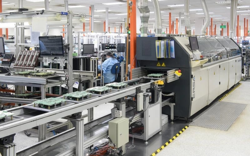
How PCB Manufacturing Begins: Materials and Layer Preparation
Most PCB manufacturing companies begin by selecting the correct materials for a project. These include copper-clad laminates, prepreg, and solder mask coatings. Material selection depends on thermal requirements, operating frequency, mechanical strength, and the environment in which the product will be used.
Once materials are chosen, teams build up the internal layers. This involves:
- Cutting and cleaning copper sheets
- Applying photoresist
- Imaging and etching trace patterns
- Aligning layers for lamination
Precise alignment is essential. Even small shifts can create open circuits, shorts, or impedance issues. Layer buildup also sets the foundation for overall board strength and signal performance.
The Role of Drilling and Plating in High-Quality Boards
After layers are laminated, companies drill holes for vias, connectors, and components. This can involve mechanical drilling or laser drilling, depending on the size and complexity of the vias. Advanced designs often use microvias, blind vias, or buried vias to save space and improve performance.
Once drilled, holes are plated with copper so current can flow between layers. This plating must be uniform. Too little copper can create reliability issues, while too much can complicate soldering or cause stress during thermal cycling.
Circuit board manufacturing companies use automated systems to measure plating thickness, inspect hole quality, and confirm that each via meets mechanical and electrical standards.
How Solder Mask and Surface Finishes Support Assembly
Before assembly begins, the board receives a solder mask layer. This coating protects the copper traces and helps prevent solder bridges during component placement. The mask must be applied evenly to avoid exposing copper or covering pads.
Surface finishes are applied next. Common choices include ENIG, HASL, OSP, and immersion silver. Each finish supports specific assembly needs:
- ENIG offers strong durability and smooth surfaces
- HASL supports cost-effective assembly
- OSP protects copper during storage
- Immersion silver supports high-frequency designs
Inspection and Testing Throughout the Build
Quality control does not exist at one single point in the process. Instead, PCB manufacturing companies conduct inspections throughout the entire build. These may include:
- Automated optical inspection (AOI)
- Flying probe testing
- X-ray inspection for multilayer boards
- Electrical testing for shorts and opens
- Visual checks for alignment and surface quality
Testing confirms that the board behaves as expected before components are added. Early detection reduces waste and helps prevent failures during final assembly.
Why Documentation and Process Control Matter
High-quality circuit board production depends on consistent, repeatable processes. Documentation ensures the same methods are used for every run, regardless of batch size or timeline. Manufacturers record details such as:
- Drill sizes
- Copper weights
- Lamination temperatures
- Solder mask thickness
- Surface finish requirements
These details help teams recreate builds accurately and track performance across different production cycles. Strong documentation also supports certifications, audits, and long-term reliability studies.
How Manufacturing Companies Support Engineers and Product Teams
Beyond fabrication, experienced companies play a hands-on role in development. Engineering teams often seek guidance on:
- DFM (design for manufacturability) improvements
- Material choices for heat or vibration
- Best practices for high-speed or RF layouts
- Via configurations for compact designs
- Stack ups that support signal integrity
This collaboration keeps projects moving forward smoothly. It also helps reduce errors that only appear during full production.
The Future of PCB Manufacturing
Circuit board technology continues to evolve. Trends include finer trace widths, higher layer counts, flexible and rigid-flex designs, and boards that support higher frequencies with less signal loss.
To meet these demands, circuit board manufacturing companies are investing in:
- Advanced imaging systems
- Laser drilling
- Automated inspection tools
- Improved materials
- Tighter process control
Final Thoughts
Reliable PCB production depends on strong processes, accurate inspections, and careful material selection. Preventing failures and supporting consistent product performance in PCB manufacturing requires structured manufacturing methods and attention to detail. MJS Designs brings both to every project, making them a dependable partner for teams that prioritize quality and precision in circuit board production.